
Introduction:
It's here.
Intel's first smartphone SoC that you'll actually be able to buy in a device
before the end of the year. The platform is called Medfield and Paul Otellini
just announced its first device partners.

Medfield
starts out as a bonafide mobile SoC. Whereas Moorestown was a
"two-chip" solution, Medfield is just one - the Penwell SoC:

Since I know
the measurements of the package I could estimate the dimensions of the silicon
itself. My math worked out to be around 62mm^2. That's larger than a Tegra
2-class SoC, but smaller than Tegra 3 or Apple's A5. The diagram of its high
level architecture above helps explain why.
There's only a single version of Medfield being
announced today: the Intel Atom Z2460. The Z2460 features a single Atom core
with a 512KB L2 cache, a PowerVR SGX 540 GPU and a dual-channel LPDDR2 memory
interface. In a world where talking about four Cortex A9s and PowerVR SGX
544MP2s isn't uncommon, Medfield starts out almost sounding a bit...tame. But
then you see its performance: 
Although
running what appears to be a stock Gingerbread browser, Intel's Medfield
reference platform posts SunSpider performance better than any other smartphone
we've tested - including the Galaxy Nexus running Ice Cream Sandwich. Intel
promises that Medfield's performance will scale on ICS as well - the gap should
be maintained. We've seen high results from reference designs in the past, but
the Medfield platform is a little different as you'll soon see - it's a
complete smartphone design that should be representative of handsets that hit
the market later this year.
Medfield
isn't a one trick pony either, performance is similarly dominating under
BrowserMark:

These are
tablet-like scores. Here the Galaxy Nexus running ICS comes close, but once
again Intel expects that on the same OS Medfield should be faster than any of
the currently available SoCs.
I asked
Intel where its SunSpider and BrowserMark performance advantages came from,
especially considering we've typically only seen huge gains with new browsers
and not new SoCs. Their response pointed to a bunch of factors, but one stand
out issue was the A9 has a great execution core but seems to be more limited on
the memory interface. Atom can support far more outstanding misses in L2 than
the Cortex A9, which chokes bandwidth to the processor for anything not already
in the L2 cache. This may be one of the reasons why we've never been able to
get really high bandwidth numbers out of A9 based SoCs. It's probably safe to
assume that things will be different with the Cortex A15, but for now it's
little things like this that give Medfield a performance advantage.
GPU
performance is understandably not as impressive. We couldn't get offscreen
numbers of GLBenchmark 2.1 but we did get results at the device's native
resolution (1024 x 600):
3D
performance is better than the OMAP 4460 due to Medfield's 400MHz GPU clock
compared to ~300MHz in most OMAP4 devices.
Performance
without power considerations is meaningless, especially in the smartphone
world. Luckily for Intel, Medfield seems very competitive there as well. Intel
provided some power and performance data for Medfield based on its reference
platform. I still haven't been able to verify any of this for myself, but I was
able to see some power tests run in person on the reference platform and
competitive devices.
The Intel
provided values are pretty astonishing . Sub 20mW idle, sub 750mW during a call
on 3G and although not pictured here, Intel's internal data suggests ~1W power
consumption while browsing the web compared to ~1.3W on the iPhone 4S and
Galaxy S 2. I've done my own measurements on 4S web browsing and came up with a
very similar value.
Standby
(3G)
|
Talk (3G)
|
Browsing
(3G)
|
Video
Playback 720p
|
|||
Apple
iPhone 4S
|
~38mW
|
~800mW
|
~1.3W
|
~500mW
|
||
Intel
Medfield Reference
|
~18mW
|
~700mW
|
~1.0W
|
~850mW
|
||
Samsung
Galaxy S II
|
~19mW
|
~675mW
|
~1.2W
|
~650mW
|
||
The performance
and power data both look great for Medfield. You would think that this data,
assuming there's nothing fundamentally wrong, would be enough to convince a
handset maker to actually give Intel a shot. You'd be right.
In addition
to disclosing Medfield performance data, Intel is also announcing partnerships
with both Motorola and Lenovo. The former is a broad, multi-year agreement
stating that Motorola plans on creating many devices based on Intel silicon -
the first of which will be a smartphone due out before the end of the year.
Tablets will follow at some point as well.
Lenovo on
the other hand will actually be taking and tweaking Intel's own Medfield
reference platform, and releasing it in China in Q2.
All of this
is exactly what Intel needed: a start.
CPU:
Medfield is the platform, Penwell is the SoC and the CPU
inside Penwell is codenamed Saltwell. It's honestly not much different than the
Bonnell core used in the original Atom, although it does have some tweaks for
both power and performance.
Almost five years ago I wrote a piece on the architecture
of Intel's Atom. Luckily (for me, not Intel), Atom's architecture hasn't
really changed over the years so you can still look back at that article and
have a good idea of what is at the core of Medfield/Penwell. Atom is still a
dual-issue, in-order architecture with Hyper Threading support. The integer
pipeline is sixteen stages long, significantly deeper than the Cortex A9's. The
longer pipeline was introduced to help reduce Atom's power consumption by
lengthening some of the decode stages and increasing cache latency to avoid
burning through the core's power budget. Atom's architects, similar to those
who worked on Nehalem, had the same 2:1 mandate: every new feature added to the
processor's design had to deliver at least a 2% increase in performance for
every 1% increase in power consumption.
Atom is a very narrow
core as the diagram below will show:

There are no dedicated integer multiply or divide units,
that's all shared with the FP hardware. Intel duplicated some resources (e.g.
register files, queues) to enable Hyper Threading support, but stopped short of
increasing execution hardware to drive up efficiency. The tradeoff seems to
have worked because Intel is able to deliver performance better than a
dual-core Cortex A9 from a single HT enabled core. Intel also lucks out because
while Android is very well threaded, not all tasks will continually peg both
cores in a dual-core A9 machine. At higher clock speeds (1.5GHz+) and with
heavy multi-threaded workloads, it's possible that a dual-core Cortex A9 could
outperform (or at least equal) Medfield but I don't believe that's a realistic
scenario.
Architecturally
the Cortex A9 doesn't look very different from Atom:
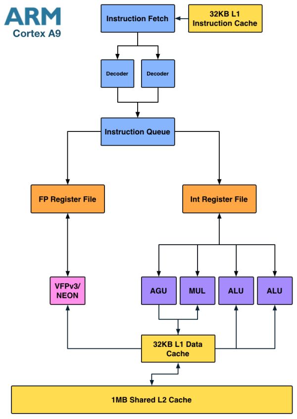
Here we see a dedicated integer multiply unit (shared with
one of the ALU ports) but only a single port for FP/NEON. It's clear that the
difference between Atom and the Cortex A9 isn't as obvious at the high level.
Instead it's the lower level architectural decisions that gives Intel a
performance advantage.
Where
Intel is in trouble is if you look at the Cortex A15:

The A15 is a far more modern design, also out of order but much
wider than A9. I fully expect that something A15-class can outperform Medfield,
especially if the former is in a dual-core configuration. Krait falls under the
A15-class umbrella so I believe Medfield has the potential to lose its CPU
performance advantage within a couple of quarters.
Enhancements in Saltwell
Although the CPU core is mated to a 512KB L2 cache, there's
a separate 256KB low power SRAM that runs on its own voltage plane. This ULP
SRAM holds CPU state and data from the L2 cache when the CPU is power gated in
the deepest sleep state. The reasoning for the separate voltage plane is
simple. Intel's architects found that the minimum voltage for the core was
limited by Vmin for the ULP SRAM. By putting the two on separate voltage planes
it allowed Intel to bring the CPU core down to a lower minimum power state as
Vmin for the L2 is higher than it is for the CPU core itself. The downside to
multiple power islands is an increase in die area. Since Medfield is built on
Intel's 32nm LP process while the company transitions to 22nm, spending a
little more on die area to build more power efficient SoCs isn't such a big
deal. Furthermore, Intel is used to building much larger chips, making
Medfield's size a relative nonissue for the company.
The die size is actually very telling as it's a larger SoC
than a Tegra 2 with two Cortex A9s despite only featuring a single core.
Granted the rest of the blocks around the core are different, but it goes to
show you that the CPU core itself (or number of cores) isn't the only
determination of the die size of an SoC.
The performance tweaks come from the usual learnings that
take place over the course of any architecture's lifespan. Some instruction
scheduling restrictions have been lifted, memory copy performance is up, branch
predictor size increased and some microcode flows run faster on Saltwell now.
Clock Speeds & Turbo
Medfield's CPU core supports several different operating
frequencies and power modes. At the lowest level is its C6 state. Here the core
and L2 cache are both power gated with their state is saved off in a lower
power on-die SRAM. Total power consumption in C6 of the processor island is
effectively zero. This isn't anything new, Intel has implemented similar
technologies in desktops since 2008 (Nehalem) and notebooks since 2010
(Arrandale).
When the CPU is actually awake and doing something however
it has a range of available frequencies: 100MHz all the way up to 1.6GHz in
100MHz increments.
The 1.6GHz state is a burst state and shouldn't be sustained
for long periods of time, similar to how Turbo Boost works on Sandy Bridge
desktop/notebook CPUs. The default maximum clock speed is 1.3GHz, although just
as is the case with Turbo enabled desktop chips, you can expect to see
frequencies greater than 1.3GHz on a fairly regular basis.
Power consumption along the curve is all very reasonable:
Medfield CPU Frequency vs. Power
|
||||||
100MHz
|
600MHz
|
1.3GHz
|
1.6GHz
|
|||
SoC Power Consumption
|
~50mW
|
~175mW
|
~500mW
|
~750mW
|
||
Since most ARM based SoCs draw somewhere below 1W under full
load, these numbers seem to put Medfield in line with its ARM competitors - at
least on the CPU side.
It's important to pay attention to the fact that we're
dealing with similar clock frequencies to what other Cortex A9 vendors are
currently shipping. Any performance advantages will either be due to Medfield
boosting up to 1.6GHz for short periods of time, inherently higher IPC and/or a
superior cache/memory interface.
GPU:
The Power VR SGX 540 in Medfield is no different from what
you'd get in an OMAP 4460, with the exception that it's clocked a bit higher at
400MHz.
The SGX 540 here is a remnant of Intel's earlier strategy to
have Medfield out far sooner than it actually is going to show up on the
market. Thankfully Intel has plans to introduce a PowerVR SGX 543MP2 based
Medfield successor also before the end of the year.
Video Decode/Encode Support, Silicon Hive ISP
Intel relies on two more IP blocks from Imagination
Technologies: the VDX385 and VDE285 for 1080p video decode and encode. Intel
claims support for hardware accelerated 1080p30 decode, High Profile. Maximum
supported bitrate is apparently up to 50Mbps, although Intel only demonstrated
a 20Mbps High Profile stream:

Medfield's ISP is provided by Intel owned Silicon Hive. The
ISP supports cameras ranging from 5MP to 16MP (primary sensor), with the
reference design standardizing on an 8MP sensor. Medfield supports burst
capture at up to 15 fps (8MP).
The Process
Intel bifurcated its process technology a few years ago,
offering both low power and high performance versions of each of its process
nodes. Today those process nodes are staggered (45nm LP after high perf 32nm,
32nm LP debuts after high performance 22nm, etc...) however Intel plans on
bringing both in lockstep.
Medfield debuts on Intel's 32nm LP process. The only details
we have from Intel are that leakage is 10x lower than the lowest on 45nm.
Compared to Moorestown, Medfield boasts 43% lower dynamic power or 37% higher
frequency at the same power level.
The bigger and more valid comparison is to TSMC's 28nm
process, which is what companies like Qualcomm will be using for their
next-generation SoCs. It's unclear (and very difficult) to compare different
architectures on different processes, but it's likely that Intel's 32nm LP
process is more comparable to TSMC's 28nm LP process than it would be to any
4x-nm node.
It is important to note that Intel seems very willing to
sacrifice transistor density in order to achieve lower power consumption where
possible. I don't believe Intel will have the absolute smallest die sizes in
the market, but I also don't believe it's clear what the sweet spot is for
mobile SoCs at this point. It's quite likely that Apple's ~120mm^2 target is
likely where everyone will eventually end up in the near term.
The Roadmap
Although Medfield is already posting competitive performance
numbers, its current competition is roughly a year old. Within the next two
quarters we'll see smartphones and tablets shipping based on Qualcomm's Krait.
The next-generation Snapdragon platform should be Cortex A15-like in its
performance level
Today we have Medfield, a single core Atom paired with a
PowerVR SGX 540 built on Intel's 32nm LP process. Before the end of the year
we'll see a dual-core Atom based Medfield with some form of a GPU upgrade. I
wouldn't be too surprised to see something like a PowerVR SGX 543MP2 at that
point either. In tandem Intel will eventually release an entry level SoC designed
to go after the more value market. Finally we'll see an Intel Atom based SoC
with integrated Intel baseband from its Infineon acquisition - my guess is
that'll happen sometime in 2013.
0 comments:
Post a Comment